- 您现在的位置:买卖IC网 > Sheet目录2006 > LTC2446IUHF#TRPBF (Linear Technology)IC ADC 24BIT 8CH HI SPEED 38QFN
LTC2446/LTC2447
7
24467fa
TEST CIRCUITS
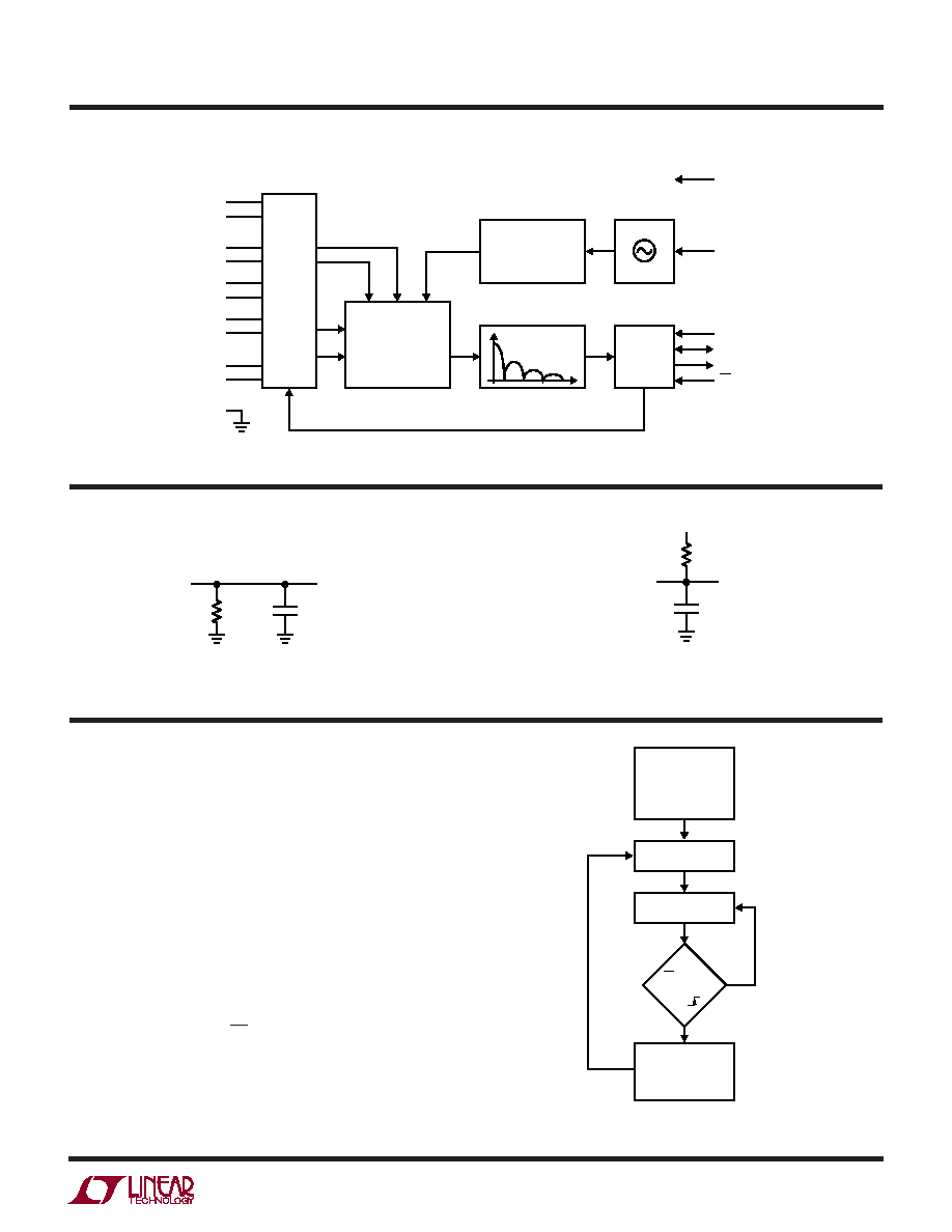
FU CTIO AL BLOCK DIAGRA
UU
W
Figure 1. Functional Block Diagram
APPLICATIO S I FOR ATIO
WU
U
CONVERTER OPERATION
Converter Operation Cycle
The LTC2446/LTC2447 are multichannel, multireference
high speed, delta-sigma analog-to-digital converters with
an easy to use 3- or 4-wire serial interface (see Figure 1).
Their operation is made up of three states. The converter
operating cycle begins with the conversion, followed by
the low power sleep state and ends with the data output/
input (see Figure 2). The 4-wire interface consists of serial
data input (SDI), serial data output (SDO), serial clock
(SCK) and chip select (CS). The interface, timing, opera-
tion cycle and data out format is compatible with Linear’s
entire family of
Σconverters.
Initially, the LTC2446/LTC2447 perform a conversion.
Once the conversion is complete, the device enters the
Figure 2. LTC2446/LTC2447 State Transition Diagram
AUTOCALIBRATION
AND CONTROL
DIFFERENTIAL
3RD ORDER
Σ MODULATOR
DECIMATING FIR
ADDRESS
INTERNAL
OSCILLATOR
SERIAL
INTERFACE
GND
VCC
CH0
CH1
CH7
COM
IN+
REF+
REF–
IN–
INPUT/REFERENCE
MUX
SDO
SCK
VREFG
+
VREFG
–
VREF67
+
VREF67
–
VREF01
+
VREF01
–
CS
SDI
FO
(INT/EXT)
24467 F01
CONVERT
SLEEP
NO
YES
CHANNEL SELECT
REFERENCE SELECT
SPEED SELECT
DATA OUTPUT
POWER UP
IN+=CH0, IN–=CH1
REF+ = VREFO1
+,
REF– = VREF01
–
OSR=256,1X MODE
24467 F02
CS = LOW
AND
SCK
1.69k
SDO
24467 TA03
Hi-Z TO VOH
VOL TO VOH
VOH TO Hi-Z
CLOAD = 20pF
1.69k
SDO
24467 TA04
Hi-Z TO VOL
VOH TO VOL
VOL TO Hi-Z
CLOAD = 20pF
VCC
发布紧急采购,3分钟左右您将得到回复。
相关PDF资料
LTC2448IUHF#TRPBF
IC ADC 24BIT HI SPEED 38QFN
LTC2451ITS8#TRPBF
IC ADC 16BIT DELTA SIG TSOT23-8
LTC2452ITS8#TRPBF
IC ADC 16BIT DELTA SIG TSOT23-8
LTC2453ITS8#TRMPBF
IC ADC 16BIT DELTA SIG TSOT23-8
LTC2482IDD#TRPBF
IC ADC 16BIT 10-DFN
LTC2483IDD#TRPBF
IC ADC 16BIT I2C 10-DFN
LTC2485CDD#TRPBF
IC ADC 24BIT I2C 10-DFN
LTC2487CDE#PBF
IC ADC 16BIT DELTA SIG 14-DFN
相关代理商/技术参数
LTC2447CUHF#PBF
功能描述:IC ADC 24BIT 8CH HI SPEED 38QFN RoHS:是 类别:集成电路 (IC) >> 数据采集 - 模数转换器 系列:- 标准包装:1,000 系列:- 位数:16 采样率(每秒):45k 数据接口:串行 转换器数目:2 功率耗散(最大):315mW 电压电源:模拟和数字 工作温度:0°C ~ 70°C 安装类型:表面贴装 封装/外壳:28-SOIC(0.295",7.50mm 宽) 供应商设备封装:28-SOIC W 包装:带卷 (TR) 输入数目和类型:2 个单端,单极
LTC2447CUHF#TRPBF
功能描述:IC ADC 24BIT 8CH HI SPEED 38QFN RoHS:是 类别:集成电路 (IC) >> 数据采集 - 模数转换器 系列:- 标准包装:1,000 系列:- 位数:16 采样率(每秒):45k 数据接口:串行 转换器数目:2 功率耗散(最大):315mW 电压电源:模拟和数字 工作温度:0°C ~ 70°C 安装类型:表面贴装 封装/外壳:28-SOIC(0.295",7.50mm 宽) 供应商设备封装:28-SOIC W 包装:带卷 (TR) 输入数目和类型:2 个单端,单极
LTC2447IUHF#PBF
功能描述:IC ADC 24BIT 8CH HI SPEED 38QFN RoHS:是 类别:集成电路 (IC) >> 数据采集 - 模数转换器 系列:- 标准包装:1 系列:microPOWER™ 位数:8 采样率(每秒):1M 数据接口:串行,SPI? 转换器数目:1 功率耗散(最大):- 电压电源:模拟和数字 工作温度:-40°C ~ 125°C 安装类型:表面贴装 封装/外壳:24-VFQFN 裸露焊盘 供应商设备封装:24-VQFN 裸露焊盘(4x4) 包装:Digi-Reel® 输入数目和类型:8 个单端,单极 产品目录页面:892 (CN2011-ZH PDF) 其它名称:296-25851-6
LTC2447IUHF#TRPBF
功能描述:IC ADC 24BIT 8CH HI SPEED 38QFN RoHS:是 类别:集成电路 (IC) >> 数据采集 - 模数转换器 系列:- 标准包装:1,000 系列:- 位数:16 采样率(每秒):45k 数据接口:串行 转换器数目:2 功率耗散(最大):315mW 电压电源:模拟和数字 工作温度:0°C ~ 70°C 安装类型:表面贴装 封装/外壳:28-SOIC(0.295",7.50mm 宽) 供应商设备封装:28-SOIC W 包装:带卷 (TR) 输入数目和类型:2 个单端,单极
LTC2448CUHF
功能描述:IC ADC 24BIT HI SPEED 38QFN RoHS:否 类别:集成电路 (IC) >> 数据采集 - 模数转换器 系列:- 标准包装:1,000 系列:- 位数:16 采样率(每秒):45k 数据接口:串行 转换器数目:2 功率耗散(最大):315mW 电压电源:模拟和数字 工作温度:0°C ~ 70°C 安装类型:表面贴装 封装/外壳:28-SOIC(0.295",7.50mm 宽) 供应商设备封装:28-SOIC W 包装:带卷 (TR) 输入数目和类型:2 个单端,单极
LTC2448CUHF#PBF
功能描述:IC ADC 24BIT HI SPEED 38QFN RoHS:是 类别:集成电路 (IC) >> 数据采集 - 模数转换器 系列:- 标准包装:1 系列:microPOWER™ 位数:8 采样率(每秒):1M 数据接口:串行,SPI? 转换器数目:1 功率耗散(最大):- 电压电源:模拟和数字 工作温度:-40°C ~ 125°C 安装类型:表面贴装 封装/外壳:24-VFQFN 裸露焊盘 供应商设备封装:24-VQFN 裸露焊盘(4x4) 包装:Digi-Reel® 输入数目和类型:8 个单端,单极 产品目录页面:892 (CN2011-ZH PDF) 其它名称:296-25851-6
LTC2448CUHF#TR
功能描述:IC ADC 24BIT HI SPEED 38QFN RoHS:否 类别:集成电路 (IC) >> 数据采集 - 模数转换器 系列:- 标准包装:1,000 系列:- 位数:16 采样率(每秒):45k 数据接口:串行 转换器数目:2 功率耗散(最大):315mW 电压电源:模拟和数字 工作温度:0°C ~ 70°C 安装类型:表面贴装 封装/外壳:28-SOIC(0.295",7.50mm 宽) 供应商设备封装:28-SOIC W 包装:带卷 (TR) 输入数目和类型:2 个单端,单极
LTC2448CUHF#TRPBF
功能描述:IC ADC 24BIT HI SPEED 38QFN RoHS:是 类别:集成电路 (IC) >> 数据采集 - 模数转换器 系列:- 标准包装:1,000 系列:- 位数:16 采样率(每秒):45k 数据接口:串行 转换器数目:2 功率耗散(最大):315mW 电压电源:模拟和数字 工作温度:0°C ~ 70°C 安装类型:表面贴装 封装/外壳:28-SOIC(0.295",7.50mm 宽) 供应商设备封装:28-SOIC W 包装:带卷 (TR) 输入数目和类型:2 个单端,单极